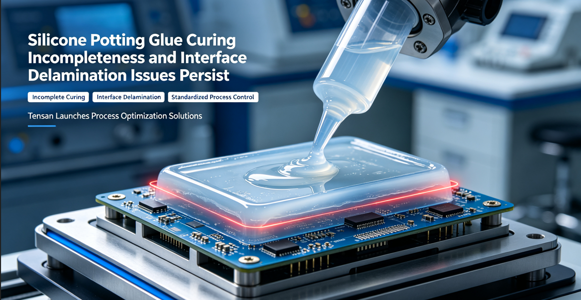



With the rapid development of the new energy vehicle, photovoltaic energy storage, and LED lighting industries, organic silicone potting glue, as a core protective material for electronic components, has seen its application scale continuously expanding. However, in actual production, in addition to common foaming issues, quality defects such as incomplete curing of the potting glue and interfacial delamination between the adhesive layer and the substrate are also troubling many manufacturers. TENSAN, drawing on years of technical accumulation and on-site service experience, has conducted in-depth analysis of the root causes of curing incompleteness and delamination, and has launched standardized operational solutions covering the entire process to help the industry improve potting quality.
Incomplete Curing: The "Uncured" Adhesive Layer Poses Significant Risks.
Incomplete curing of potting glue manifests as a tacky surface, insufficient hardness, poor elastic recovery, and in severe cases, a fluid-like state. This problem is particularly prominent in low-temperature winter environments or thin-layer potting scenarios.
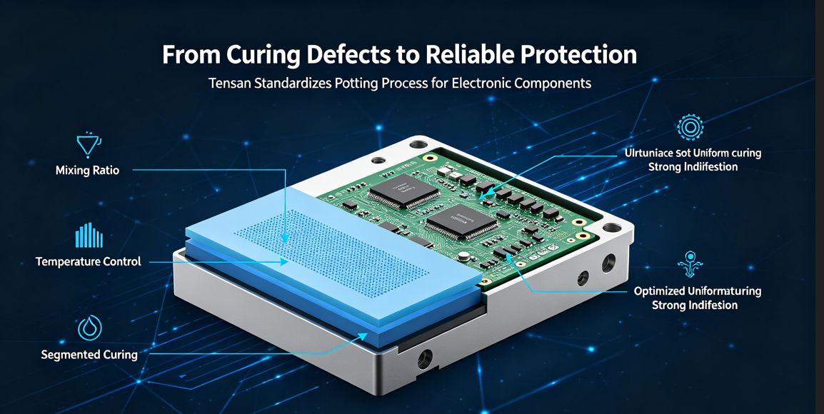
TENSAN's technical team points out that the main causes of incomplete curing include: Incorrect mixing ratio — the deviation of the A and B component mixing ratio exceeds the allowable tolerance, resulting in insufficient crosslinking reaction; Inadequate mixing — manual stirring or insufficient length of the static mixing tube leads to local concentration imbalance; Low temperature — when the ambient temperature falls below 15°C, the crosslinking reaction rate drops significantly, and curing time is prolonged exponentially; Excessively thin adhesive layer — when the thickness is less than 1mm, the reaction exotherm cannot be effectively retained, making it difficult to sustain the heat required for complete curing.
In addition, the catalyst activity in expired adhesives decays significantly, and even with the correct mixing ratio, sufficient crosslinking cannot be achieved.
Interface Delamination: Loss of Adhesion Leads to Protection Failure
Interface delamination between the adhesive layer and the PCB board, power devices, or housing is another high-frequency quality issue. Once delamination occurs, visible gaps appear between the adhesive layer and the substrate, allowing moisture and contaminants to penetrate along the gaps, leading to reduced insulation resistance, accelerated electrochemical corrosion, and ultimately module failure.
TENSAN categorizes the causes of delamination into the following aspects:
TENSAN Standardized Process Solutions
To address the above issues of incomplete curing and delamination, TENSAN has proposed systematic process improvement measures:
Material Customization and Usage Specifications
For high-reliability application scenarios, TENSAN can provide adhesion-enhanced organic silicone potting glue formulations, which incorporate special coupling agents to enhance chemical bonding between the adhesive layer and various substrates including metals, plastics, and ceramics. For products sensitive to thermal stress, low-shrinkage slow-curing systems can be selected to reduce delamination risk from the material side.
Meanwhile, Tensan reiterates that adhesive storage management should not be overlooked. The FIFO (First-In, First-Out) principle should be strictly implemented, and expired products are strictly prohibited from use. Adhesives must be fully returned to room temperature before use to prevent condensation caused by temperature differences between cold adhesive and hot substrates, which could otherwise lead to poor interfacial wetting.
Industry Trend: Process Refinement Determines Protection Reliability
As the automotive electronics and energy storage systems place increasingly stringent requirements on long-term reliability, potting processes have evolved from simple "pour and wait for curing" to comprehensive refined management covering material selection, pretreatment, proportioning and mixing, curing process control, and post-treatment. The standardized process system advocated by TENSAN is providing electronic manufacturing enterprises with quantifiable and replicable operational models, helping the industry transition from "experience-driven" to "standard-driven," and laying a solid foundation for the high-quality development of the new energy and automotive electronics industry chain.